Application Field
Thermal Interface Materials for Telecom & Data Center
Engineered for 24/7 uptime across 5G infrastructure, optical modules and data center servers. Sheen TIMs fill micro-gaps, stabilize interface contact and support repeatable manufacturing at scale.
Lower interface thermal resistance
Gap & pressure window
Cycling / aging stability
Silicone-free options
Why Telecom & Data Center Designs Overheat
5G base stations, radios, and network equipment operate continuously under heavy processing and RF loads, and overheating can drive failures, performance degradation, and higher energy consumption. Data center servers are “always on” and thermal management choices are closely tied to reliability and energy efficiency.
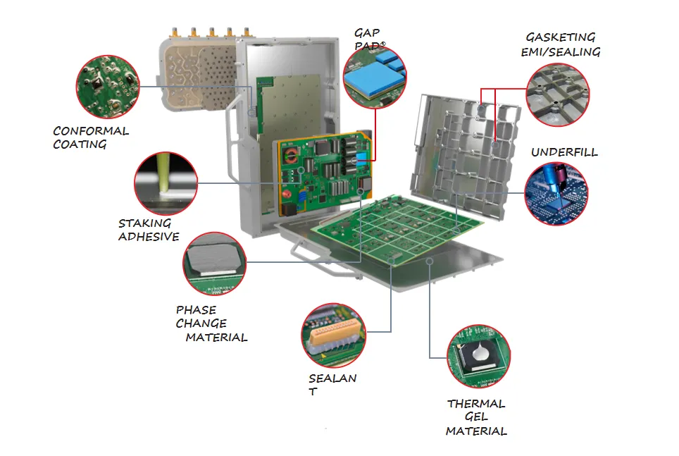
Procurement-friendly deliverables: clear spec ranges, thickness window, die-cut availability, and a sample plan aligned with your validation workflow.
Key Platforms & Hotspot Locations
Platform → Component → Interface → Material Choice
5G Base Station / Radio Unit
Hotspots: baseband processors, RF power amplifiers, DC-DC modules, enclosure thermal paths.
pad
gel
tape
Optical / Fiber Modules
Hotspots: lasers, driver ICs, cages/heatsinks; contamination control may require silicone-free solutions.
silicone-free
pad
putty/gel
Servers / AI Nodes
Hotspots: CPU/GPU/accelerator, VRM, memory; interfaces to heatsink or cold plate (air or liquid cooling).
pcm
grease
pad
Networking (Routers/Switches)
Hotspots: ASIC/SoC, PHY, power stages; focus on controlled thickness and repeatable placement.
pad
die-cut
gap control

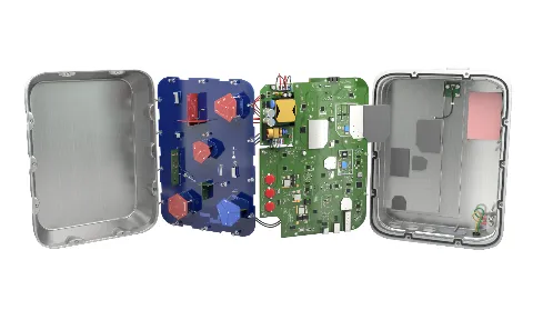
Outdoor Access Point
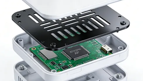
Indoor Access Point
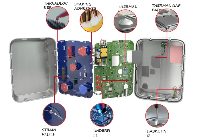
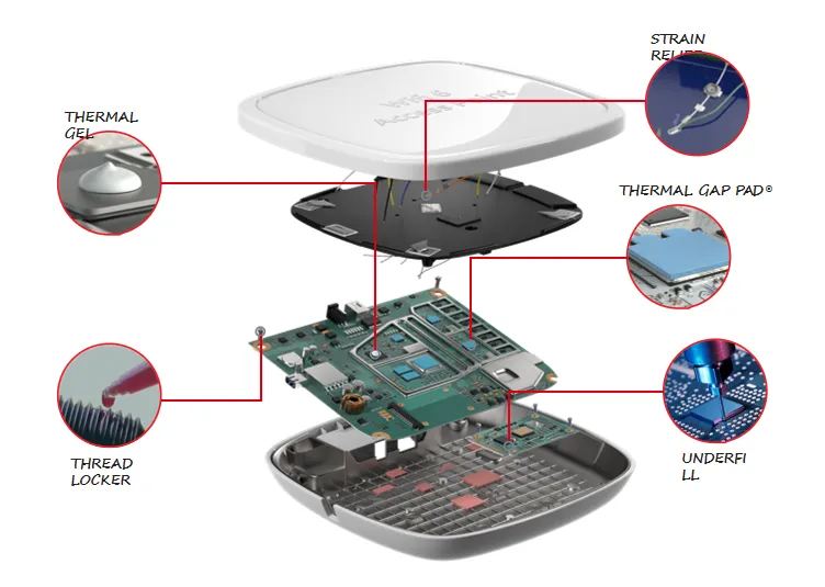
.
Product Parameter Matrix (Quick Comparison)
Designed for fast sourcing decisions: material family → conductivity range → thickness window → typical use.
| Material Family | Thermal Conductivity | Thickness Window | Best Fit in Telecom / Data Center | Manufacturing Notes |
|---|---|---|---|---|
| Silicone Thermal Pad | 1.5–15.0 W/m·K | 0.3–10.0 mm | ASIC/VRM/PA modules → heatsink/chassis; routers & switches | Fast placement; can be supplied as sheets or die-cut parts |
| Silicone-Free Pad | 1.0–6.0 W/m·K | 0.5–5.0 mm | Optics/transceivers & silicone-sensitive zones | For contamination control requirements, confirm service temperature |
| Thermal Gel (SE20–SE100) | 2.0–10.0 W/m·K | Process-defined | PSU/power modules with uneven profiles; complex gap variation | Dispensing/screen printing/spreading; supports automation |
| Phase Change Material (PCM) | 1.8–8.0 W/m·K | 0.13–0.5 mm | CPU/GPU/ASIC → heatsink/cold plate (thin interface) | Activates near operating temperature; clean handling options |
| Thermal Grease | 1.0–5.0 W/m·K | Min 0.05 mm | High-pressure thin bond line CPU/GPU interfaces | Process control + rework strategy recommended |
| Carbon Fiber Thermal Pad | 15–45 W/m·K | 0.3–12.0 mm | Performance-driven designs with defined thermal path direction | Confirm mechanics & interface pressure; shortlist recommended |
Need a datasheet shortlist? Send: platform, interface type, min/max gap, pressure window, target temperatures, silicone restriction, and production method. We’ll respond with recommended grades and sample plan.
Telecom & Data Center
Use this section to match your interface geometry
and the assembly process with the most stable material family
and the assembly process with the most stable material family
Telecom & Data Center
Continuous high-load operation drives temperature spikes if interfaces are not well controlled. Goal: stable contact, controlled compression, and repeatable assembly.
-
Primary choices: Silicone Pads (gap filling) / Thermal Gel (uneven profiles)
-
Secondary choices: Tape/adhesive for bonding where mechanical fixation is limited
-
Deliverables: die-cut shapes, thickness window, compression control plan
Telecom & Data Center
Routers, SSD modules, graphics thermal modules, and other compact electronics where fast placement is preferred.
| Component | Interface | Recommended | Notes |
|---|---|---|---|
| SoC → heatsink/spreader | Stable contact | Confirm gap distribution & compression | Confirm pressure & flatness; manage rework strategy |
| Memory/VRM → chassis | Handle tolerance | Softness helps cover unevenness | Handle tolerance; avoid over-compression |
| SSD controller → enclosure | Coupling | Balance thickness vs pressure | Gel for uneven profiles; pad for speed & thickness |
Remote Radio Heads
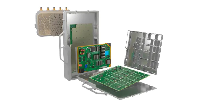
Base Stations
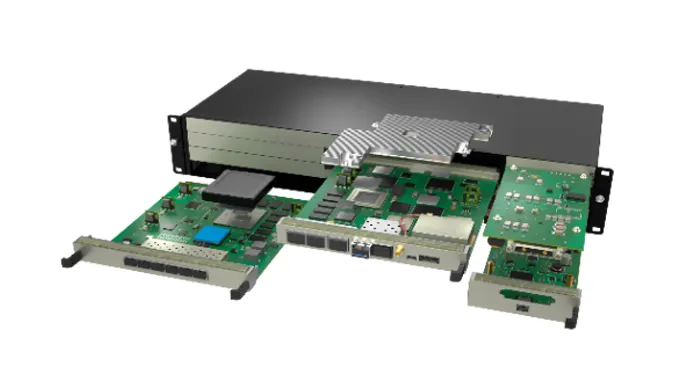
Fixed Wireless Arrays
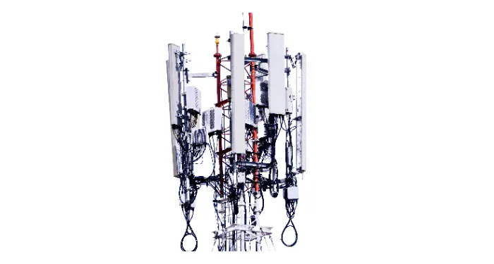
Telecom & Data Center
Real Customer Case Data
Outdoor 5G RU
-
Challenge: continuous load, wide ambient range, enclosure heat path.
-
Interface: PA/DC-DC modules → chassis/heatsink.
-
Recommended: soft pads (controlled compression) + gel for uneven profiles.
Optical Transceiver Zone
-
Challenge: thermal control near optical components with contamination constraints
-
Interface: module/cage → spreader/heatsink.
-
Recommended: silicone-free pads; consider gel/putty for geometry variation.
-
Procurement notes: silicone restriction confirmation, service temperature, die-cut shapes.
1U/2U Server Node
-
Challenge: thin bond-line CPU/GPU interfaces, rework strategy, consistent assembly.
-
Interface: CPU/GPU/accelerator → heatsink/cold plate.
-
Recommended: PCM or grease for thin interfaces; pads for VRM/memory coupling.
-
Procurement notes: application method control, thermal cycling validation, and documentation for sourcing.
Validation Checklist
A simple, repeatable approach for engineering qualification. Keep documentation consistent for procurement review.
What TIM is typically used for 5G base station power modules?
Soft pads are commonly used for defined gaps and rapid placement; gels are preferred when the profile is uneven or the gap variation is large. Final choice depends on gap mapping and allowable pressure.
When should I specify silicone-free for optical modules?
If the design includes silicone-sensitive optics/transceivers or contamination-controlled zones, silicone-free pads can be shortlisted early to reduce risk. Confirm service temperature and cleanliness requirements.
PCM vs. Grease for Server CPU/GPU: How to Choose?
Both support thin bond lines. PCM can provide process-friendly handling near operating temperature; grease fits ultra-thin interfaces when application method and rework are controlled.
Do you supply die-cut parts and thickness options?
Yes. Die-cut shapes and thickened windows help improve assembly consistency and reduce operator variation—useful for both engineering validation and volume procurement.
What information is required for a recommendation?
Platform, interface type, min/max gap, pressure window, thermal targets, silicone restriction, and production method (placement/dispensing/printing). Add drawings and a power map for the fastest turnaround.
Stabilize temperatures for 24/7 uptime
Submit your gap range, pressure window and thermal targets. We’ll reply with recommended material families, spec ranges and a sample plan.